


Easy Search, Quick Enquiry
In CGM, You no need to register to initiate an inquiry for interesting products.
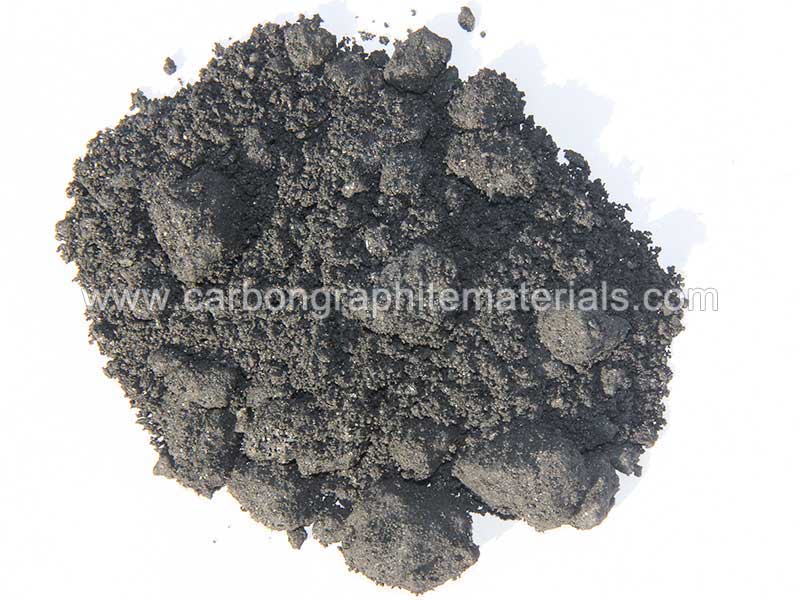
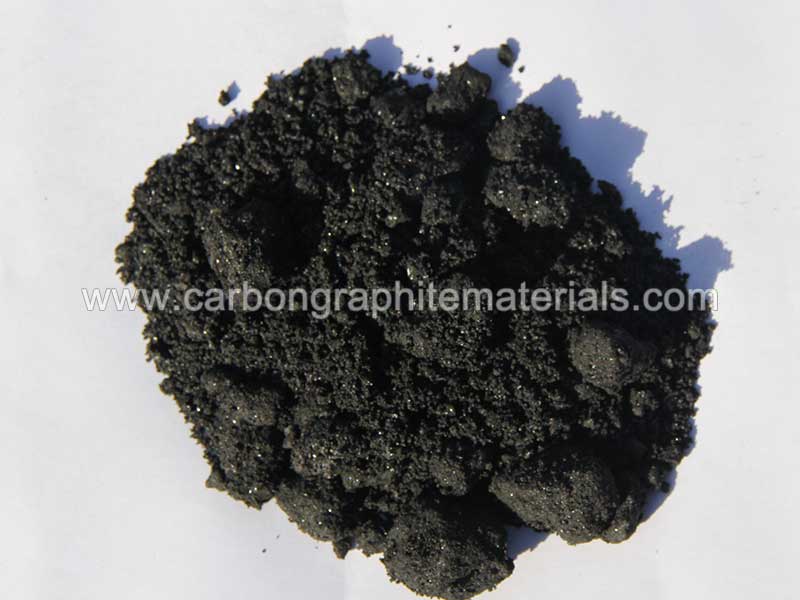
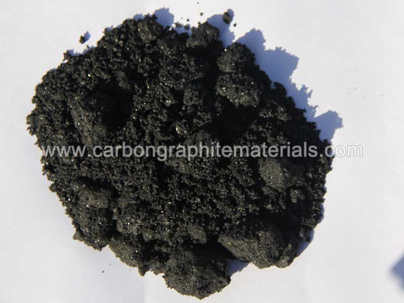
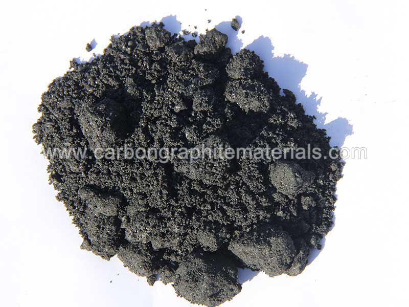
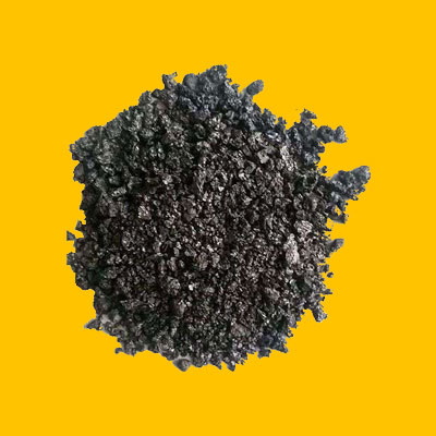
Graphite means that the molecular structure of carbon products is changed and arranged regularly by high temperature or other means. This molecular arrangement makes the molecular spacing of carbon wider, which is more conducive to decomposition and nucleation in molten iron o...
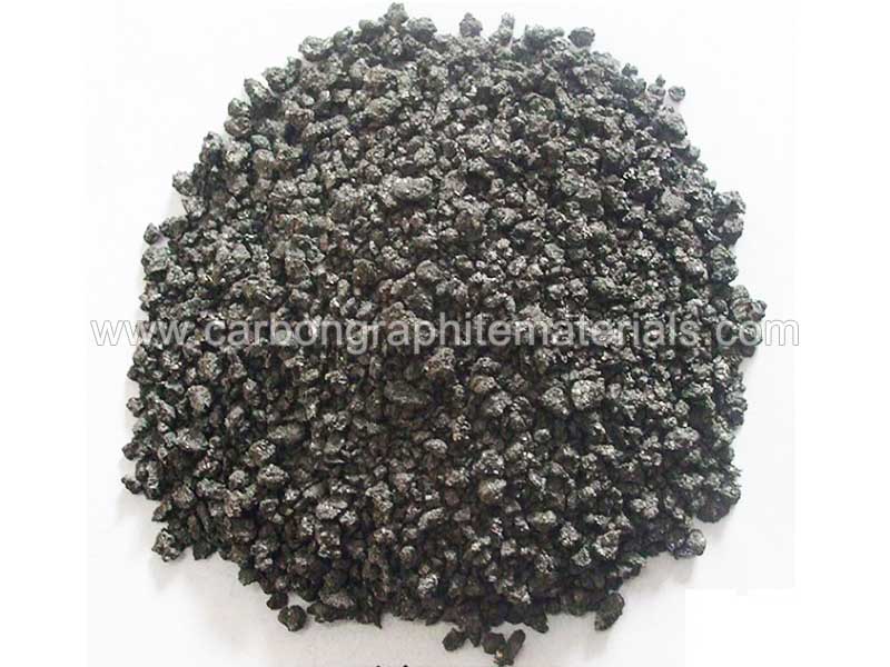
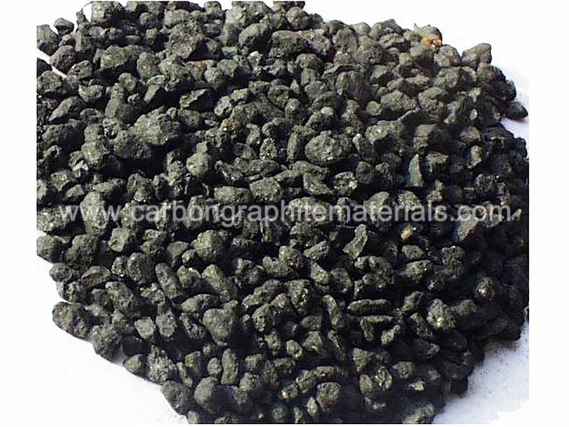
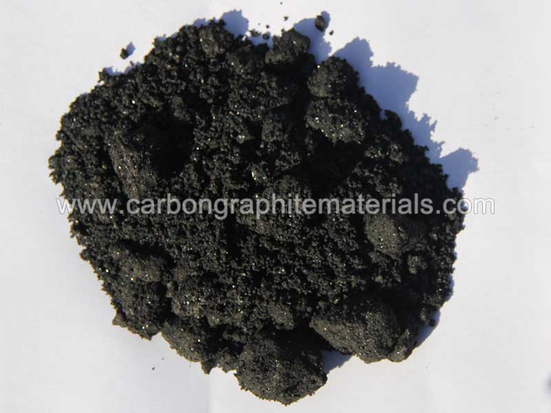
The same chemical composition uses different melting processes, different compositions and proportions, the metallurgical quality of molten iron is completely different, and good carburization effect is obtained. The electric furnace uses carbon enhancement technology, and the...
The graphite heater shall be inspected and managed in the early stage before use, otherwise, the graphite heater may explode during use. The following should be done: 1. First of all, check whether the graphite heater has cracks in the early stage of work. If there are no crac...
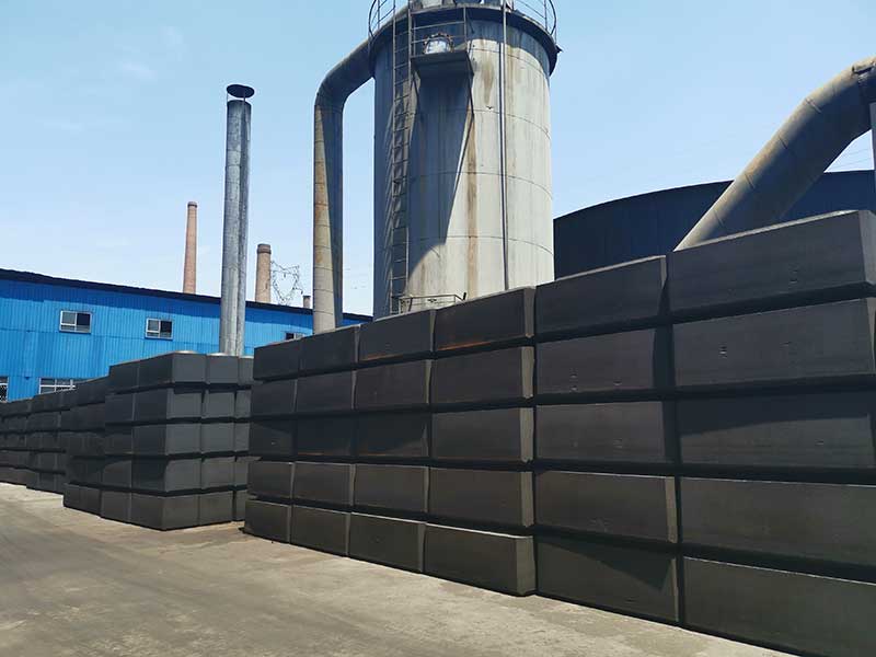
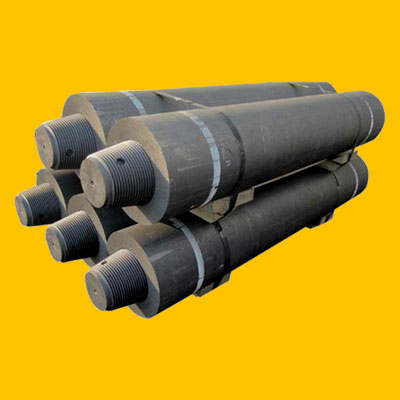
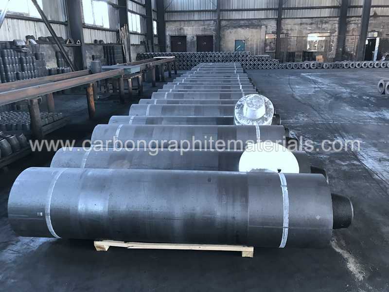
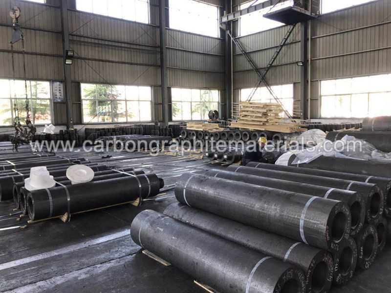
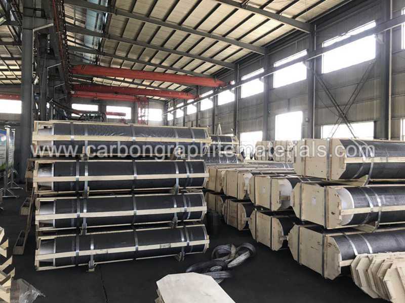
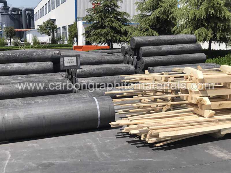
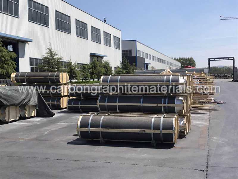
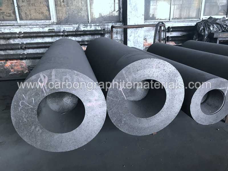
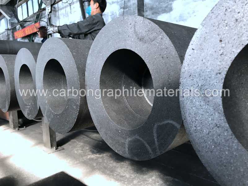
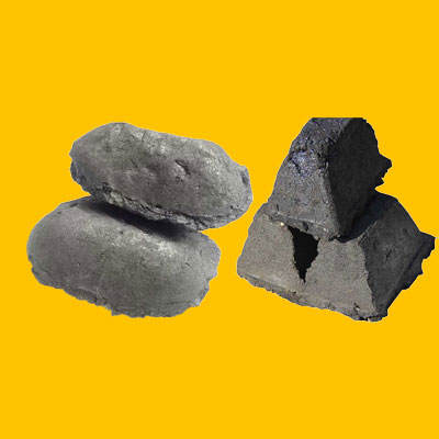
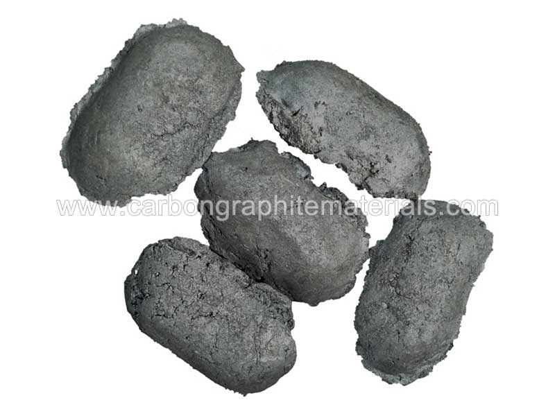
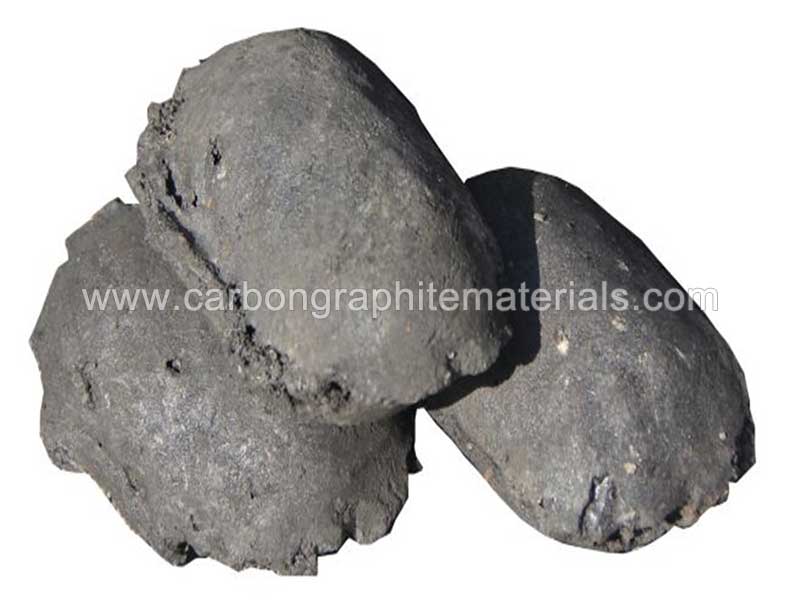
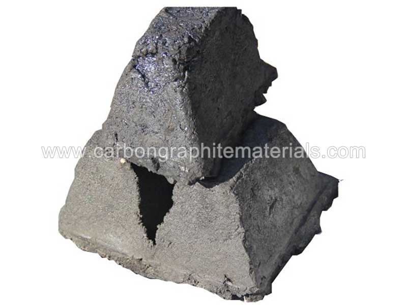
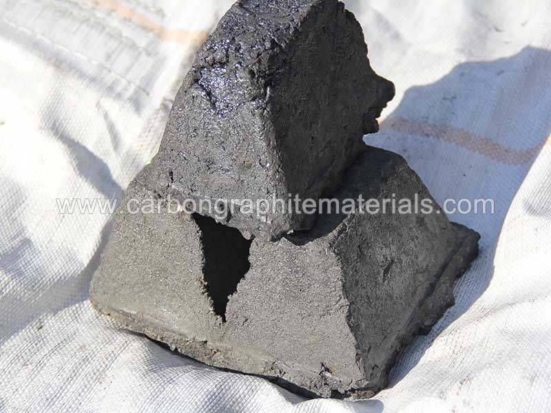
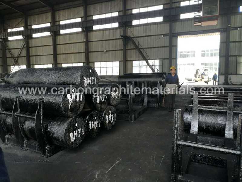
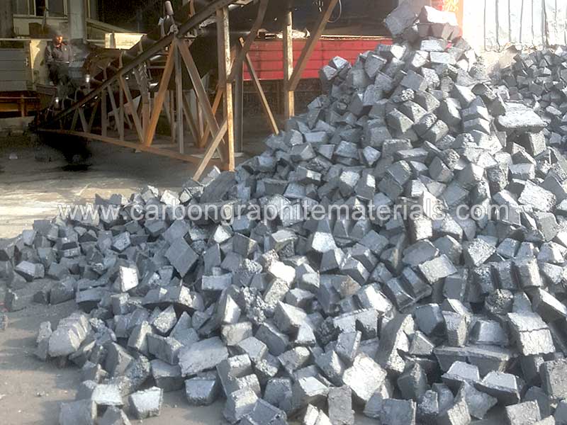
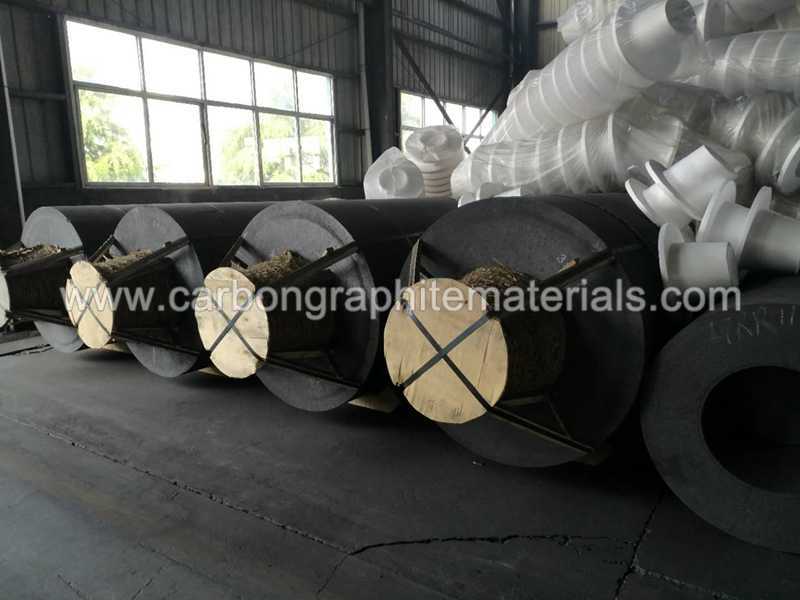
The mechanical strength of electrode paste includes compressive strength, flexural strength and tensile strength The height of the electrode paste refers to the height from the upper end of the electrode clamp to the top end of the electrode paste. If the electrode paste is to...
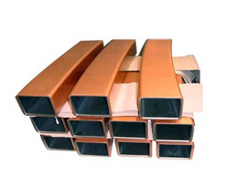
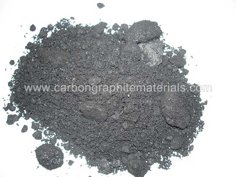
Expanded graphite is a product of deep processing of graphite. Expanded graphite can be used to produce packing rings, various types of gaskets, and can also be directly pasted on various metal surfaces to effectively solve gas-phase sealing. Expanded graphite has good corrosi...
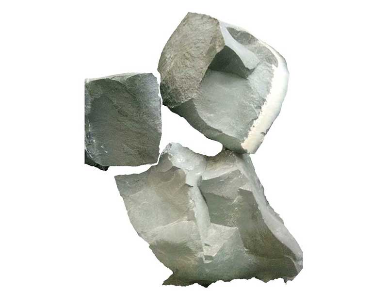
Silicon carbide is a kind of synthetic carbide with molecular formula of SiC. It is usually formed of silicon dioxide and carbon at a high temperature of 2000. D egree. Density: the particle density of various silicon carbide crystal forms is very close, which is generally con...